Artistic PCB Design for Terrified Beginners workshop
Hello and welcome to Artistic PCB Design for Terrified Beginners
If you're not familiar with some of those concepts:
- PCBs stands for Printed Circuit Boards, the things that electronic devices are build on
- Art means people creating wonderful (or awful) things for other people to enjoy
- A terrified beginner is someone who we all either are or have been at some point
I'm Kliment, and I'm doing this workshop to achieve one or more of the following things:
- Get art people to play with electronics
- Get electronics people to play with art
- Give the two groups above a common language so they can talk to each other
- Get people to build something cute and have fun
We're going to be making a so-called "Shitty addon". A shitty addon is a small circuit board that gets attached as a decorative or functional addition to one of the many badges that are so popular at hacker events. We're going to make one that doesn't do much (except light up). Except it won't be shitty! It will be pretty! So let's call it a pretty addon!
Workflow and prerequisites
What you're going to need to be able to follow along. Please make sure the following software is installed and working on your computer *BEFORE YOU START*.
- Kicad 5.1.x ( https://kicad-pcb.org/ ) - an awesome free and open electronics CAD software package
- Inkscape (any version https://inkscape.org/ ) - an awesome free and open vector drawing software package
- Krita (any version https://krita.org ) - an awesome free and open art creation and image editing software package
I made an hour-long video where I explain a bit about what PCBs are and what they're made of and go through the process of converting graphics to PCBs.
It's at https://www.youtube.com/watch?v=9oVzUmkM5-0 and you can watch it right now, or during the workshop, up to you. If you watch it beforehand that's fine.
I've put some materials for you at: https://github.com/kliment/artpcb/ which you can download at https://github.com/kliment/artpcb/archive/master.zip
Very broadly, here's what we're going to do:
- Create art
- Create PCB from art
- Generate manufacturing files from our PCB and optionally have it manufactured
- Enjoy your new superpowers
Techniques
Step One: Create, borrow, or steal art
I can't help you a whole lot with this one, except the borrow/steal bit. I've put some pictures you can use in the workshop materials. Feel free to use those! Alternatively, bring your own photos, drawings, sketches, whatever. Scribble something on some paper and photograph it. Doesn't matter, as long as it's a picture you like. Make sure this is in one of two formats:
- Vector drawing that Inkscape can read (ideally svg) OR
- A raster image format like PNG or JPG or something else that Krita can read
Step Two: Create PCB from art The main thing to understand when converting art to a circuit board is that circuit board manufacturers and PCB design software doesn't think in art - it's designed for making circuit boards that meet their functional technical requirements. We do still care about functional requirements, but we mostly care about how it's going to look. So, we need to understand the PCB as the manufacturers and design software sees it, so we can adapt our art to that. So from now on, we're thinking in layers and manufacturing processes.
Here is what happens when a circuit board is made (very roughly):
- The manufacturer takes a big sheet of fiberglass with thin layers of copper either side. (note: fiberglass is beige-brown, translucent. Copper is metallic and opaque.)
- A bunch of holes are drilled into the sheet, and some nasty chemistry is applied to cover the inside walls of the holes with more copper
- The copper is printed over with an acid-resistant material in a pattern we provide (front and back copper layer)
- All the copper that is not part of the pattern is dissolved away
- The board is covered with a thin layer of paint in a specific color. This is called soldermask. The paint is removed in a pattern we provide (front and back mask layer). Note that any place that has the mask removed will expose either copper or fiberglass.
- The board gets printed with another ink, usually white (unless you have white soldermask, in which case it's black). This is called silkscreen and is printed in a pattern we provide (front and back silkscreen layer).
- The board gets a "surface treatment" to prevent corrosion of any exposed copper - this is normally either HASL or ENIG. HASL stands for Hot Air Solder Leveling - it's the cheapest process. The entire board gets dipped into molten solder, and then a blade of really hot air passes across the board and blows the molten solder away, leaving the surface mostly level. HASL surface finish is silver in color, and slightly uneven, giving you a moon-like surface of reflective metal. ENIG is a more expensive process that deposits a microscopically thin layer of nickel and then an even more microscopically thin layer of gold on top of the copper. This gives you a perfectly flat, slightly matte gold surface wherever you have exposed copper. You don't get to choose where the surface treatment goes - it gets applied to all exposed copper.
- The board gets some more holes drilled into it, and then it gets milled - a rotating blade that looks a lot like a drill bit goes around the shape of the board and cuts it from the sheet. The shape of the board is something we provide - however the milling bit is fairly large (about the size of the fat end of a sharpie) so we can't have any inside corners with sharp angles.
So here are the things that we need to provide the manufacturer:
- Board outline (what shape the board should be milled into)
- Copper layers (where they should leave the copper on)
- Mask layers (where they should take the soldermask off)
- Silkscreen layers (where they should print silkscreen)
- Drill file (where we want holes to go, and whether they should be filled with copper or not)
Luckily, our PCB design software can do most of the work for us, but we still need to tell it what we want on there. Now, PCB design software works with slightly different concepts. Here's what we have available:
- Component footprints - combination of holes and copper patterns and mask openings and silkscreen that are combined together and can be moved and placed as a whole
- Traces - lines in the copper that electrically connect various things
- Copper pours - shapes that get filled with copper, optionally connected electrically to something on the board
- Keepout areas - shapes that prevent copper pours and traces from entering them
- Mask and silkscreen lines and polygons - shapes that create openings in the mask layer, or add paint to the silkscreen layer
- Board outline - a bunch of lines that form a closed shape that defines the shape of the board
- Imported raster art - this goes on either the mask layer, creating an opening there, or on the silkscreen layer
Inkscape - vector drawings and board outlines
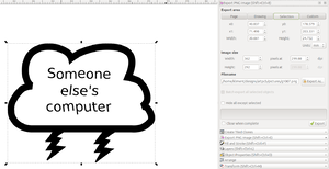
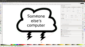
Before we get to the PCB design software, let's start with graphics software. First, I'll show you how to take an Inkscape vector drawing, export it for a mask opening or silkscreen, and make a matching board outline. Open up Inkscape and load up your image. Select your image, go to Export PNG Image in the area to the right of your image, and click "selection". Scale your image until it has the size you want (you can select mm or inch as units). Write down the dpi value you used (300 is fine). Click "export as" and put in a file name. Click "export".
Try this out with the cloud, snake, and bladder images provided. (hehee, snakes and bladders, I know, I'm sorry)
(if you just want to stick your logo or drawing on an existing PCB, you're done, you can skip the next bit)
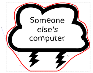
Now, use the "draw bezier curves and straight lines" tool

click around the shape you have, forming a rough outline, and make sure it's closed (the last click is on the first node):
Select your new path, go to "fill and stroke" and set the stroke color to something that is clearly different from your image.
Now, use the edit path tool

and drag on the segment between each node to create handles. Drag the nodes and handles until you have a nice shape.
Make sure there are no sharp inside corners - imagine you need to draw the shape with the fat end of a sharpie:
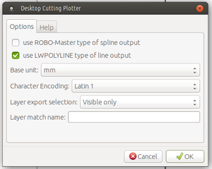
Next, select your base image and delete it, leaving just the path. Now, go to File->Save a Copy and select "Desktop Cutting Plotter (AutoCAD DXF R14)" as the format. Give the file a name ending in .dfx
Hit Ctrl-Z (Option-Z on mac) to undo the delete.
Now you have exported an image at a particular size and a board outline. Great! Now what if you don't have a nice vector image but are starting with a photograph or a sketch?
Using Krita to convert a photo to soldermask or silkscreen graphics
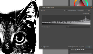
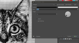
An important thing to understand about imported raster art is that anything we import will be turned into a binary image - either black or white. We can't work with shades of grey - there's no way to manufacture those. There are several ways of converting shades of grey to black and white. We'll look at two methods - the threshold method and the halftone method. The threshold method turns every pixel that is darker than a particular value black and all the other pixels white. The halftone method creates circles of different size corresponding to the brightness of each area in the image. Thresholding is a better method for sharp lines and clearly defined features, halftone gives much better results for shades of grey and soft blurry areas.
Here is an example of the difference between thresholding and halftone:
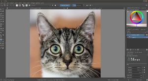
Here's how to do this in Krita: Load up the image:
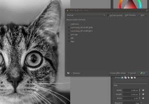
Use Filter->Adjust->Desaturate to turn the image to greyscale:
Now, use one of the following tools: Filter->Adjust->Threshold (adjust the threshold level to your liking):
or Filter->Artistic->Halftone (adjust the dot size and angle to your liking):
Then do a File->Export and save it as a PNG. If you just want to put a picture on the PCB, you're done for now. If you are using an image to fill the entire board, export again after the next step.
Krita - outlines
In the layers panel on the right, create a new vector layer and switch to it. Set the brush size (top panel) to something small, like 4pixels. Set the color to something that contrasts with your image. Use the bezier curve tool to add some points around the image. Make sure that the last and first points match. Drag the segments and handles around to make a board outline. See the instructions for making a board outline in inkscape above. When you're happy with it, use Layer->Export->Save vector layer as SVG. Now go to Select->Convert to Vector Selection and then Select->Invert Selection. Switch back to the layer with your original image and press delete. You should be left with just the part of the image inside the outline.
Open up Inkscape and File->Open the SVG file you just created. Select the path, and click on "Export PNG Image" in the right panel. Switch units to mm or in. Scale the image until it is the correct size for the board you want, as reported by width/height in the "export PNG image" panel. Write down this size, you will need it later. Then use "File->Save a Copy" and select "Desktop Cutting Plotter (AutoCAD DXF R14)" as the format. Give the file a name ending in .dfx
Working in KiCAD
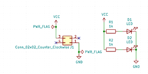
Because we want our PCB to also have a function (in this case, it has two light-emitting diodes that light up) we are going to add some components and connect them together. To keep track of what is connected to what, we have a schematic. In our case, we won't be doing much with the schematic - you can leave it as-is.
Aside: wtf is a schematic? A schematic is a drawing, a bit like a flowchart, that tells you what parts are in an electronic thing and how they are connected to each other. Our schematic is extremely simple - it has a four-pin connector, two resistors and two LEDs. The connector plugs into one of many hacker event badges, and two of its pins provide power to our board. This power flows through the resistors, and through the LEDs. When our addon board is connected to a badge, the LEDs will light up, and their brightness will depend on the value of the resistors. Here is our schematic:
Each component on the schematic becomes a footprint on the PCB, and each line on the schematic becomes a trace on the PCB. I've already mapped the components to footprints for this, but if you want to use different parts instead feel free to do so. To make changes to the schematic, open kicad, open the project, and double-click on the schematic:
To change what parts are on your board, use this button:
But it's perfectly okay to stick with the parts that are already there - they're 0805-size LEDs and resistors, and they are big enough to solder by hand comfortably. When we're ready with the schematic, we can switch to the PCB. Use this button to do so:

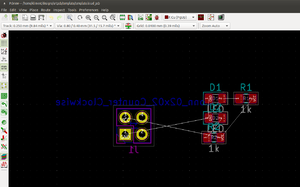
So here we are in our PCB editor:
That's all we need from the electronics point of view. Now, we're going to add a board outline, some elements on the mask layer, and some elements on the silkscreen.
Use File->Import->Graphics to import the outline dxf you saved earlier with inkscape - make sure you put it on layer Edge.Cuts so KiCAD knows it's your board outline. Place it so the 4-pin square connector is approximately bottom center. Press Alt-3 to see a 3d view of your board. If it looks right, that's great. If the size seems off, you can resize in inkscape, save it again, and import it again, after using undo in the pcb editor.
Now, let's make a footprint library and add our graphics to it:
Create a folder called art.pretty (it can be called anything as long as it ends in .pretty - "art" is nice because it ends up near the top of any alphabetical list).
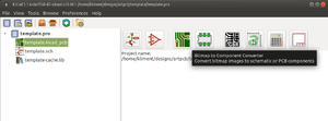
In the kicad main window, click the "bitmap to component converter" button:
Load up your picture, and change the two resolution boxes to match the size you want the thing to have on your board. Select either silk screen or solder mask, and export the new part into your art.pretty directory.
In your PCB editor, go to preferences -> manage footprint libraries, go to project specific libraries tab, click the folder icon and find your art.pretty directory.
Then click OK, press the O button on your keyboard, click on the board, and find the category called "art" in the resulting window. Place the image where you like it. You can use the Move command (press M while pointing to the part) or the Rotate command (R) or the Flip command (which moves things from front to back of board and vice versa). Use the 3D Viewer (Alt-3) to see your work.
If you added an image on the mask layer, you will notice it doesn't get filled with gold/copper. If you want that, you will need to add some copper areas to the board. Use the "add filled zones" tool for this  . Keep the default zone settings to completely fill the zone with copper without connecting it to anything. Draw a zone around the outside of your board. Exact shape doesn't matter as long as your entire board is inside it. Double click to close the zone. Then press B to recalculate all shapes in the zone. Check the result on the 3D viewer.
If you want to remove copper from a zone, use the keepout areas tool (just below the add filled zones tool). Deselect tracks and vias and select copper pours. After you are done with your shape press B again.
Place your components using Move (M), Flip (F) and Rotate (R) keys. I recommend placing LEDs and resistors on the reverse of the board (flipped) so you can use the board as a diffuser or have backlit features. Place your parts so the thin white lines that are connecting them don't cross.
Now it's time to route the traces between components. If you placed the parts with no white lines crossing, this is easy. If you placed your components on the back of the board, use the pagedown key to switch to that layer, and then press X to enter routing mode. Click on each pad, then move the mouse to wherever the white line takes you, and click again. This will create a trace. Make sure all the white lines have been replaced by traces before you continue.
You can add lines, polygons, circles and text on the silkscreen or mask layers if you like (though it's usually easier and more fun to do this in inkscape or krita).
If you want to add some holes, either add circles on the Edge.Cuts layer (for holes without copper), or use the via tool (for holes with copper).
When done, press B and then Alt-3 to look at your board.
When you're happy with what you've got, you can export the board for manufacture.
Exporting for manufacture
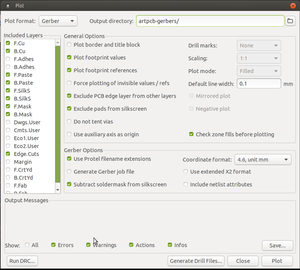
Go to File->Plot. Use these settings:
- Click "Generate Drill Files".
- Click "Generate Map File".
- Click "Generate Drill File".
- Click "Close".
- Click "Plot".
- Click "Close".
You now have a directory of "gerber" files that any PCB manufacturer can work with. Zip it up and you can send it to manufacture!
